2012年11月29日星期四

The Mini Project


  We have completed all the 6 experiments in 3810, and now we are focusing on the final project.It is called the mini project since all we have done will present just on the PCB board.Now let me introduce the idea of our project.
    Have you ever played the Race Game before. The racer drives his car and run as far as he can. He will meet many obstacles on the road.If he doesn't touch this obstacles he will continue to get more points.But if he touch the obstacles, game over.What we want to do this time is using a keypad and a LCD and the chips to design a single race game.
  I believe everyone has played the game above. Yeah, it is called the Russian Blocks.I think the rule of this game can be just stated as a single sentence:
  Who can not let the block touch the top of the screen for a longer time, who will get more marks.
  We don't do the Russian Blocks this time, so why I'm talking about the Russian Blocks? What I want to tell you is that we want to use this blocks to form a car.
  How to make this become true? We need the Graphic LCD and the assembly language.

The Graphic LCD 128*64

   Maybe you are wandered how we can form a car buy using these blocks.How can let the blocks formed as what we want. The answer is, using the Assembly Language to program the code.

The Control Instruction Of Graphic LCD

  For example, if you want to show a letter "S" on the LCD, you should use the assembly language put the command into the chip, and you should always provide the position of each blocks.Each column has 8 blocks, which is the length of a byte. Each bit can be set "1" or "0" to represent its light on or off.The lowest block stands for the MSB. For example, we can use a series of bytes to represent 'S'.That is :
00100110b = 26h
01001001b = 49h
01001001b = 49h
01001001b = 49h
00110010b = 32h  
00000000b = 00h     (from left to right and dismiss the first two columns)
  We want to design the initial starting interface on LCD.So we use the software to draw these black blocks.The software is Graphic Gales.If we want to design our car it is very helpful to use these.And if we print it out, it will help us to do the programming.
Use the Graphic Gales to design the logo


The Assembly language


Then we put the code into the compiler,we can see the logo we designed on the LCD.
WATCH OUT BIRDS!!


  What we have uploaded is just the result we have done. We need to continue our procedure.So good luck to us, and I will share the fun this game gives us on the blog!!


2012年11月8日星期四

Experiment 5 Interface of the 8088 MPU with 8254 PTC and 8255 PPI


  How time flies.Now we have to do the experiment 5.This course requires us to do 6 Experiment and 1 mini project.So you see ,we don't have many chances to do experiment.The last four experiments makes me know better about the Microprocessor and the function of the chips.So I have a confidence to do this experiment well.

  In this experiment ,our mission is to write the program in Assembly language,then we have to program this in the chips to control the LEDS and the buzzer.
8254A Programmable Timer Controller

The position of 8254A in PCB
  Since we have to know the basic knowledge of Assembly Language,we have to study how to get the meaning of a example code in the Experiment,which is a huge task.It is not the same as C language,and we have not use Assembly Language to make a program.
The program in Assembly Language
  There is always a question which confuses me for a long time,that is how the assembly language can make the chips in the CPU work.Why a series of ‘0’‘1’can command the computer to do so many things.Actually ,Assembly Language is fun.

Assembly Language is fun
  We have talked about the background of the Experiment 5 for such a long time,and now I will come back to the subject.Before we put the code into the chips, we have to wrap the wires to the certain pins of the chips ,just as the  photo in left side shows: 


  To be honest, it is not easy to connect the pins with wires, you have to concentrate because once you connected the wrong chips it will cost you much time to debug.And you have to make the length of the wire properly,either too long or too short wires may lead to error.
Tools for wrapping wires
You have to use the tools to remove the insulator.


  Then we wrap the metal part of the wires in the pins.And make sure we have to rotate clockwise.If you have made a mistake, you change the other side of the stick and rotate again.
  After the wrapping ,you may get a PCB like this:

Sample of the wrapped PCB
  Now let's come back the program,you just use the software to put your exe5.bin file into the 8254A,and connect the PCB to the power,you will get the result.


  This experiment is prepared for my final mini project, and I find that we have to be careful in each details.It is worthy for us to spend more time on the wrapping.Although it may cost more time ,but it will save time in debugging.Debug can make people crazy.And I think I should know more about the Assembly Language.


Reference::                           IERG 3810 Lab Mannul

2012年10月17日星期三

Use of Logic Analyzer for State Analysis


  After the last two experiments,I have some feeling about doing experiment.The moment that I get the result is unforgettable , and I really enjoy this moment.
Today I will do the Experiment 3,Use of Logic Analyzer for State Analysis.Through this experiment I want to study the use of logic analyzer for state analysis , and study the program with disassembler in state analysis.
Before the experiment, I have to understand what is the state of microprocessor ,which is illustrated as left:


  And we have to let compiler know how to arrange the structrue,so we  have to define a code segment.

Define a code segment at 0F800H

This is the first time that I contact with the assemble language, it is a basic language for the computer, and through the assembly we can translate the assemble language into the machine language.

EPROM(Erasable programmable Read Only Memory)

After finishing the language in the computer ,we have to put the code into the EPROM.EPROM s a type of memory chip that retains its data when its power supply is switched off. In other words, it is non-volatile. It is an array of floating-gate transistors individually programmed by an electronic device that supplies higher voltages than those normally used in digital circuits. Once programmed, an EPROM can be erased by exposing it to strong ultraviolet light source (such as from a mercury-vapor light). EPROMs are easily recognizable by the transparent fused quartz window in the top of the package, through which the silicon chip is visible, and which permits exposure to UV light during erasing.
  Then we put the EPROM in the prototype board and then we will get the result soon.


1.Connect the POD1 and POD3 with the PCB circuit.

 2.Program for USB EPROM Emulator


3.Load configuration files. ET8088_A._E, I8088

4.Format, assign pins.

5.Set trigger condition.


 Then we have get the result just showing in the below:

The result of the experiment

The result of the experiment

  During the experiment we have known how to use logic analyzer for state analysis.And we have felt the powerful effect of assembler language.From the operand we know what the cpu is doing in the current time.And we also know what the real meanings are for the operands such as “MOV” ”JUMP” ”LOOP”.Although we have just contacted the assembler language, the experiment can provide us with a background for us ,which is benefit for us further study.
  I have just known a little bit about Microprocessor,and what I have done is just the follow the steps, which comes from the teacher.I have no idea about the coming mini project. But I have talk to my senior sister(師姐),she told me don't worry about that. I have to read the textbook more carefully to let the knowledge more solidly.  


Referencehttp://en.wikipedia.org/wiki/EPROM
          2012exp3_state_analysis(2012.09.27).pdf 


2012年9月24日星期一

Tough Task1--Microprocessor System Design Laboratory


IERG 3810
(Microprocessor System Design Laboratory) )is the first lab course in CUHK.And since I have never attend the lab in CUHK before, I feel curious about it ,and of course ,a little bit nervous.

  My lab course is at 2:30 p.m in Tuesday afternoon, my friend who has attended the class on Monday told me that he had not finished the experiment in the lab time .He reminded me that I should start the experiment as early as I can with my partner Wu.Oh,no,we have to face challenge again in the evening.


The Shaw Run Run Science Building
  
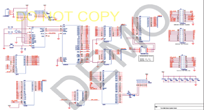
  The first experiment is Schematic Drawing and PCB Design,i even dont know the meaning of PCB design since I didt do any circuit design in the lab before.The software OrCAD, I even dont hear about it.I console myself that the first experiment will be easy, but the moment I open the demo.pdf,Im shocked. 


The Circuit Diagram we have to draw
  Why Im shocked? Because I even dont know what the logo of OrCAD it is,and complete the job on OrCAD is one part of this experiment. Oh...


I'm crazy

(Crazy......)
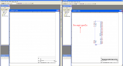
 But the bad feeling disappears rapidly as soon as I find the two other document. The content in the document tells us step by step about what should we do firstly,secondly, etc. Each step gives us a picture to show clearly.For example:
  

  Even I dont anything about OrCAD, I can achieve my aim to draw a circuit diagram as the demo shows through the procedure in pdf.

  During the experiment,my partner and I take turns to work. Each person works for 45 minutes and then the other will continue,which guarantees the efficiency.
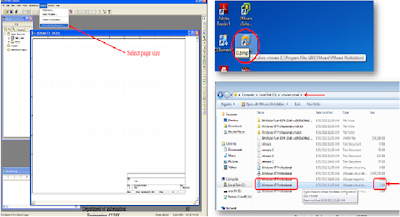
Open The OrCAD


Draw Circuit Device
  I think the most troublesome problem is searching for the proper component.There are so many component in the software and I cant find the component I need in a short time.I have a discuss with my partner , and finally we have figure out the function in the software that we can input the first letter of the components name,and then we will find the proper component soon.
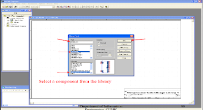

Search The Proper Circuit Device


  That night, we have worked for nearly 4hours to complete the first mission of Lab 1, I have never experience working in the midnight in the mainland,but here ,in ERB1007,I feel excited when I finally get the result.I even dont feel tired.
  In the next day ,we continue doing the second process--lay out.It means we have to make the circuit diagram we have done suitable for PCB design.(In the demo we have seen that all the devices are not connected with wires,but after lay out,it looks like a real PCB design.) Just as what the PDF says, finally we get the result:
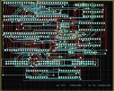

The Circuit Diagram After Lay Out

  Do you think that the first experiment is over ?Oh no, half of the mission has been done. I need to do the experiment report.The English report is not just as the same as Chinese report.Since the teacher doesn't say anything about the report.I have to search the comments on the Internet. A English report contains the 7 parts which are listed in the below:
1.Abstract
2.Introduction
3.Method
4.Results
5.Discussion
6.Conclusion
7.Reference
And finally,I got the report:
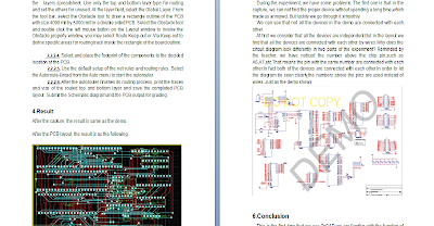


The Experiment Report
 
 The experiment has already taken us about 7 hours to finish it, we have never felt such an amazing feeling before.It gives us an opptunity to construct the concept of Information Engginering,practise the skills of using software,which is important for us.